
Scalable quantum photonic devices
relies on the efficient and controlled generation of single photons for processing and exchanging quantum information across different nodes in a solid-state or hybrid quantum network.
One of the main advantages of a solid-state platform is the possibility to integrate emitters such as semiconductor quantum dots (QDs) with nanophotonic circuits in a single chip, to build scalable quantum information processing devices [1].
A challenging task in this direction is to scale photonic devices to perform experiments involving several quantum bits (or qubits) [2].
In the quantum photonics group, we are developing a circuit platform for scalable quantum photonic technologies using gallium arsenide (GaAs) waveguides (see nanofabrication page).
Our research on scalable quantum photonic devices focuses on various aspects:
Numerical simulation of nanophotonic structures
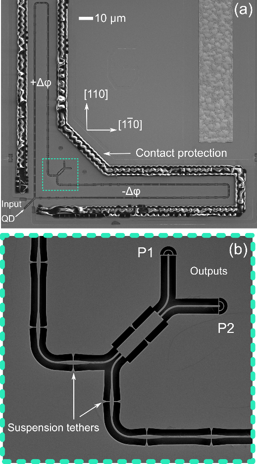
An integrated electro-optic switch fabricated on free-standing GaAs waveguides capable of routing single photons from an embedded QD emitter [2].
Nanophotonic structures can be efficiently simulated using the finite element method (FEM) or finite difference time domain (FDTD) algorithms. Numerical simulations provide insight into the optical properties of a device before fabricating it.
By solving Maxwell equations in complex dielectric geometries, we can estimate important quantities relevant for quantum photonic devices, such as the coupling efficiency of an emitter, the local density of optical states (LDOS), the transmission efficiency and scattering loss of a device, quality factors of resonators, etc…
Active routing of single photons in a circuit
The combination of a QD and an electrically-controlled switch is a key building block for quantum photonics as it allows routing individual photons into separate channels (de-multiplexing) to realize Nx1-photon resources.
This is very challenging as it requires fast (sub-μs), small-footprint, broadband, and low-loss switches operating at cryogenic temperatures (< 10 K).
Such technology is being developed in our group thanks to the advanced fabrication processes developed over the last 5 years. We developed a compact cryogenic switch using the electro-optic effect in GaAs [3].
We are also pursuing nano-opto-electro-mechanical switching as an alternative to the electro-optic effect [4].
Efficient chip-to-fiber coupling
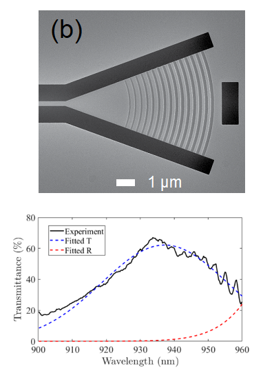
High-efficiency and low-reflectivity grating coupler (>65%) for coupling light in- and off-chip using fibers or optical objectives [5].
Quantum photonic circuits require an efficient interface to optical fibers for coupling light in and out of the chip or performing measurements with an external detection apparatus.
Due to the small dimension of dielectric waveguides (200-300 nm) compared to the optical fibers (5-10 um), spot-size converters are required. We are developing highly-efficient strategies for the out-coupling based on various approaches.
These involve evanescent coupling to nanofibers [5], gratings [6], and tapers for end-fire coupling [7].
Group members involved in scalable quantum photonic devices: Xiaoyan Zhou (Postdoc), Ying Wang (PhD), Asli Ugurlu (PhD), Camille Papon (Research assistant).
MSc projects on numerical simulation, design, and characterization of scalable quantum photonic devices are available.
For further information and details about possible projects, please contact Assistant Prof. Leonardo Midolo (midolo@nbi.ku.dk) or Prof. Peter Lodahl (lodahl@nbi.ku.dk).
[2] P. Lodahl, Scaling up solid-state quantum photonics, Science 362, 646 (2018).